
Absolute Maximum Ratings
Parameter | Unit | Min. | Typical | Max. | Notes |
Storage Temperature | °C | -40 | 85 | ||
Operating Relative Humidity | % | 0 | 85 | ||
Power Supply Voltage | V | -0.5 | 3.63 | ||
Damage Threshold | dBm | 5 |
Recommended Operating Conditions
Parameter | Unit | Min. | Typical | Max. | Notes |
Operating Case Temperature | °C | 0 | 70 | 1 | |
Power Supply Voltage | V | 3.135 | 3.3 | 3.465 | |
Power Supply Current | A | 1.6 | |||
Power Consumption | W | 5 | |||
Pre-FEC Bit Error Ratio | 2.4E-4 | 2 | |||
Post-FEC Bit Error Ratio | 1E-12 | 2 | |||
Bit Rate | Gbps | 212.5 |
Note:
1.Case Temperature here is depending on module case around TOSA, please do remember it is NOT the environmental temperature .
2.FEC is provided by host system.
Electrical Characteristics
Parameter | Unit | Min. | Typical | Max. | Test point1 | Notes |
Transmitter | ||||||
Signaling Rate per lane (range) | GBd | 26.5625 ± 100 ppm | TP1 | |||
Differential pk-pk Input Voltage Tolerance | mVpp | 900 | TP1a | 2 | ||
Differential Input Return Loss | dB | Equation (83E-5) | TP1 | |||
Differential to Common Mode Input Return Loss | dB | Equation (83E-6) | TP1 | |||
Differential Termination Mismatch | % | 10 | TP1 | |||
Module Stressed Input Test | See 120E.3.4. 1 | TP1a | 3 | |||
Single-ended Voltage Tolerance Range | V | -0.4 | 3.3 | TP1a | ||
DC Common Mode Voltage | mV | -350 | 2850 | TP1 | 4 | |
Receiver | ||||||
Signaling Rate per lane(range) | GBd | 26.5625 ± 100 ppm | TP4 | |||
Differential pk-pk Output Voltage Tolerance | mVpp | 900 | TP4 | |||
AC Common-Mode Output Voltage, RMS | mV | 17.5 | TP4 | |||
Differential Output Return Loss | Equation (83E-2) | TP4 | ||||
Common to Differential Mode Conversion | Equation (83E-3) | TP4 | ||||
Differential Termination Mismatch | % | 10 | TP4 | |||
Transition Time, 20% to 80% | ps | 9.5 | TP4 | |||
Near-end ESMW (Eye Symmetry Mask Width) | UI | 0.265 | TP4 | |||
Near-end Eye Height, Differential | mV | 70 | TP4 | |||
Far-end ESMW (Eye Symmetry Mask Width) | UI | 0.2 | TP4 | |||
Far-end Eye Height, Differential | mV | 30 | TP4 | |||
Far-end Pre-cursor ISI Ratio | % | -4.5 | 2.5 | TP4 | ||
DC Common Mode Voltage | mV | -350 | 2850 | TP4 | 4 | |
Note:
1.The location of TP1 , TP1a and TP4 are defined in IEEE 802 .3bs Figure 120 E–5 and Figure 120 E–6.
2.With the exception to IEEE 802 . 3bs 120 E .3. 1 .2 that the pattern is PRBS31Q or scrambled idle.
3.Meets BER specified in IEEE 802 .3bs 120E. 1. 1.
4.DC common mode voltage generated by the host. Specification includes effects of ground offset voltage .
Optical Characteristics
All performance is defined over the recommended operating environment unless otherwise specified.
Parameter | Unit | Min. | Typical | Max. | Note |
Transmitter | |||||
Signaling Rate, each lane | GBd | 26.5625 ± 100 ppm | |||
Modulation Format | PAM4 | ||||
TX Central Wavelength | nm | 840 | 850 | 860 | |
Spectral Width (RMS) | nm | 0.6 | 1 | ||
Average Launch Power, each lane | dBm | -6.5 | 4 | ||
Outer Optical Modulation Amplitude ( OMAouter) , each lane | dBm | -4.5 | 3 | 2 | |
Transmitter and Dispersion Eye Closure for PAM4 (TDECQ) , each lane | dB | 4.5 | |||
TDECQ – 10 log10(Ceq)c , each lane | dB | 4.5 | 3 | ||
Average Launch Power of OFF Transmitter, each lane | dBm | -30 | |||
Extinction Ratio, each lane | dB | 3 | |||
Optical Return Loss Tolerance | dB | 12 | |||
RIN12 OMA | dB/Hz | -128 | |||
Encircled Flux | >86% at 19 um <30% at 4.5 um | 4 | |||
Receiver | |||||
Signaling Rate, each lane | GBd | 26.5625 ± 100 ppm | |||
Modulation Format | PAM4 | ||||
RX Central Wavelength | nm | 840 | 850 | 860 | |
Damage Threshold | dBm | 5 | 5 | ||
Average Receive Power, each lane | dBm | -8.4 | 4 | 6 | |
Receive Power (OMAouter), each lane | dBm | 3 | |||
Receiver Reflectance | dB | -12 | |||
Stressed Receiver Sensitivity (OMAouter)), each lane | dBm | -3.4 | 7 | ||
Receiver Sensitivity (OMAouter), each lane | dBm | Equation ( 138–1) | 8 | ||
Conditions of Stressed Receiver Sensitivity Test: | 9 | ||||
Stressed Eye Closure for PAM4 ( SECQ) , lane under test | dB | 4.5 | |||
SECQ – 10 log10(Ceq)f ( max) , lane under test | dB | 4.5 | 3 | ||
OMAouter of Each Aggressor Lane | dBm | 3 | |||
LOS Assert | dBm | -20 | |||
LOS De-Assert | dBm | -8 | |||
LOS Hysteresis | dB | 0.5 | |||
Note:
1.RMS spectral width is the standard deviation of the spectrum.
2 .Even if the TDECQ <1 .4 dB, the OMA ( min) must exceed this value.
3.Ceq is a coefficient defined in IEEE802 . 3bs 121 .8.5.3 , which accounts for the reference equalizer noise enhancement.
4.If measured into type A1a .2 or type A1a .3 , or A1a .4 , 50 μm fiber, in accordance with IEC 61280-1-4.
5. The receiver shall be able to tolerate , without damage, continuous exposure to an optical input signal having this average power level on one lane. The receiver does not have to operate correctly at this input power.
6. Average receive power, each lane (min) is informative and not the principal indicator of signal strength. A received power below this value cannot be compliant; however, a value above this does not ensure compliance.
7 .Measured with conformance test signal at TP3 (see IEEE802 .3 cd-2018 138.8. 10) for the BER specified in 138.1.1.
8.Receiver sensitivity is informative and is defined for a transmitter with a value of SECQ up to 4.5 dB.RS = max(6.5 – SECQ–7.9) (dBm) Equation ( 138–1) where RS is the receiver sensitivity SECQ is the SECQ of the transmitter used to measure the receiver sensitivity The
normative requirement for receivers is stressed receiver sensitivity.
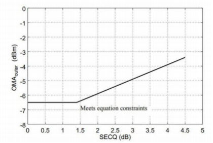
Figure1: Illustration of receiver sensitivity
9. These test conditions are for measuring stressed receiver sensitivity. They are not characteristics of the receiver.
